

Αγορά BGA Rework Station
1. You can buy BGA Rework Station direct from original manufacturer.2. DH-A2 Automatic BGA Rework Station.3. Micrometer for BGA angle adjust and motherboard adjust.4. Port: Shenzhen.
Περιγραφή
0 �% a0 Buy BGA Rework Station


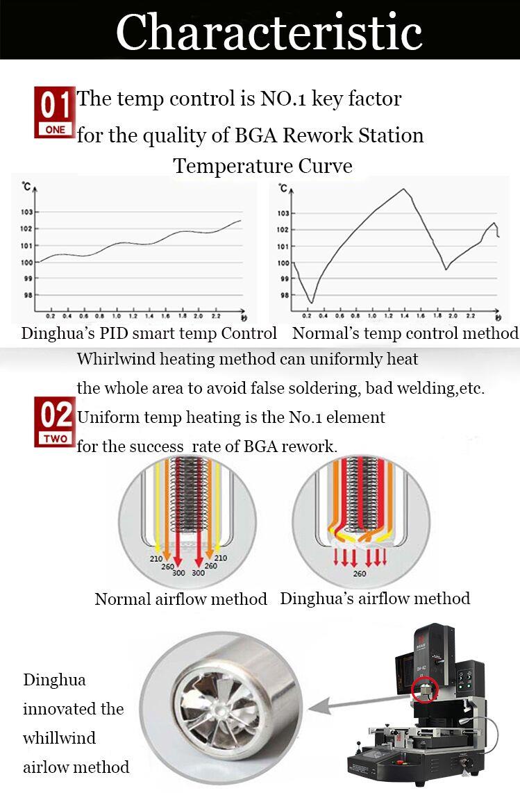
1.Application Of Automatic Optical BGA Rework Station
Εργασία με όλα είδη μητρικές πλακέτες ή PCBA.
Συγκόλληση, reball, αποκόλληση different είδος of chips: BGA,PGA,POP,BQFP,QFN,SOT223,PLCC,TQFP,TDFN,TSOP,
PBGA,CPGA,LED τσιπ.
2.Product Features of Αυτόματο Οπτικό BGA Rework Station

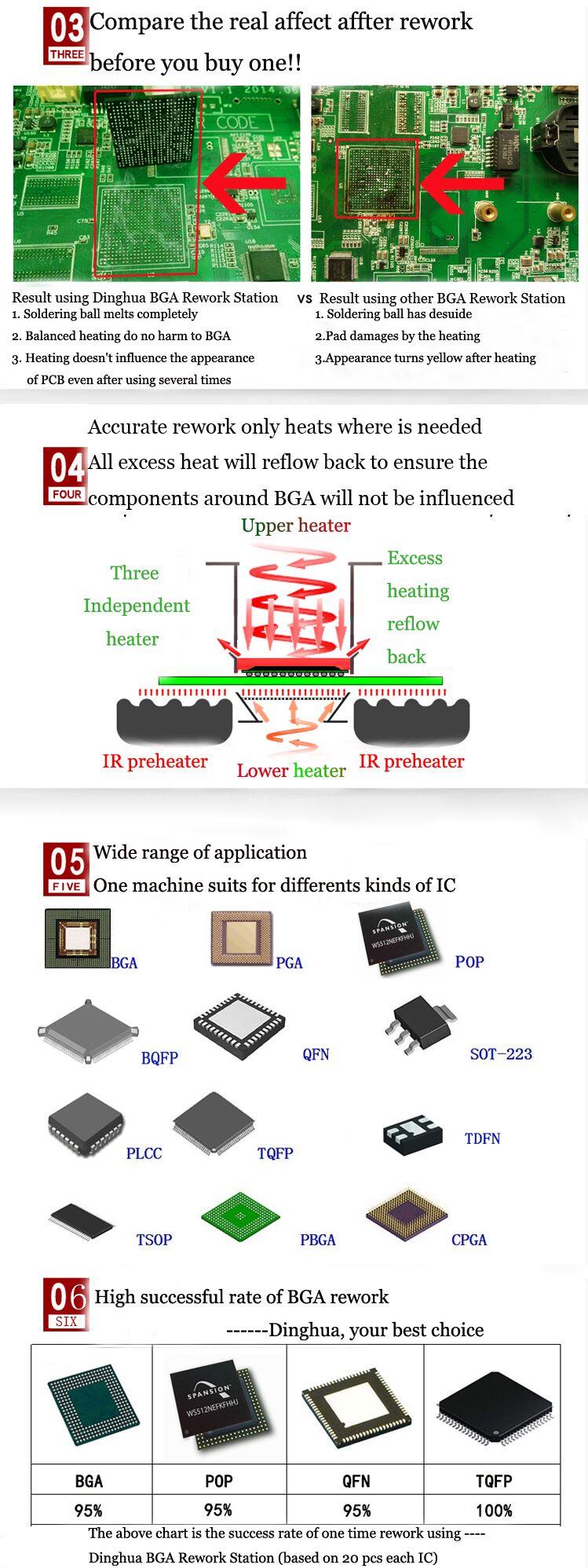
3.Specification του Αυτόματο Οπτικό BGA Rework Station

4.Λεπτομέρειες του Αυτόματο Οπτικό BGA Rework Station


5.Γιατί Επιλέξτε Μας Αυτόματο Οπτικό BGA Rework Station?
6.Πιστοποιητικό του Αυτόματο Οπτικό BGA Rework Station
UL, E-MARK, CCC, FCC, CE ROHS certificates. Εν τω μεταξύ, to improve and perfect the quality system,
Dinghua has passed ISO, GMP, FCCA, C-TPAT on-site audit certification.

7.Packing & Shipment of Αυτόματο BGA Rework Station
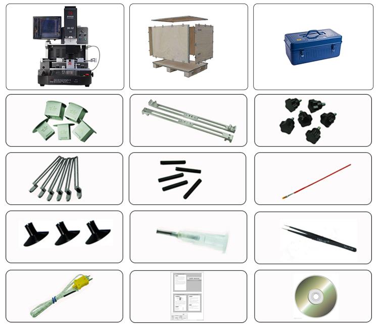
8.Shipment for Αυτόματο Οπτικό Reballing BGA Machine
DHL/TNT/FEDEX. If you want other shipping term, please tell us. We will support you.
9. Όροι Πληρωμή
Τράπεζα μεταφορά% 2c Δυτική Ένωση% 2c Πίστωση Κάρτα.
10. Πώς DH-A2 Αυτόματο BGA IC Reballing Machine work?
11. Σχετικά γνώση
Πληροφορίες flash τσιπ
Προσφορά δυναμική
Πρόσφατα, SandForce's new owner chip company LSI said that they are developing a new firmware for the SF master SSD
SSD και ταχύτητα up the startup. speed.
παράμετρος
3. 3V ισχύς παροχή;
Το εσωτερικό μνήμη κελί πίνακας του το τσιπ is (256M + 8.192M) bit × 8bit, and the data register and buffer memory are both
(2k + 64) bit × 8bit;
I/O θύρα με οδηγίες/address/data πολυπλεξία;
Ευχαριστώ to το αξιόπιστο CMOS μετακίνηση πύλη τεχνολογία % 2c το τσιπ μπορεί επιτύχει a μέγιστο 100kB πρόγραμμα % 2ferase κύκλος % 2c το οποίο % c2% a0
Εγγυήσεις δεδομένα αποθήκευση για 10 χρόνια χωρίς απώλεια.
Κατάσταση εργασίας
I/O0~I/O7: data input and output port, I/O port is often used for input of instruction and address and input/output of data,
όπου δεδομένα είναι
Enter during the reading process. When the chip is not selected or cannot be output, the I/O port is in a high σύνθετη αντίσταση κατάσταση.
CLE: The instruction latch is used to activate the instruction to the instruction register path and latch the instruction on the
άνοδος άκρη από WE και CLE είναι υψηλό.
ALE: Address latch, used to activate the path of the address to the internal address register, and the address is latched on the
άνοδος άκρη από WE και ALE είναι υψηλό.
CE: Chip Selector, used to control device selection. When the device is busy, CE is high and ignoed, and the device cannot return
προς το αναμονή κατάσταση.
RE: Read enable, used to control the continuous output of data and send the data to the I/O bus. The output data is valid only on
το πτώση άκρη του του RE, και it μπορεί επίσης συσσωρευτεί εσωτερικό δεδομένα διευθύνσεις.
WE: The write enable terminal is used to control the instruction writing of the I/O port. At the same time, the command, address
και δεδομένα μπορεί be μανδάλωση on the rising edge of the WE pulse through this port.
WP: Write protector, which can be write-protected in the power conversion through the WP terminal. When WP is low, its internal
Υψηλό επίπεδο γεννήτρια θα είναι επαναφορά.
R/ B : Ready/Busy output, the output of R/B can show the operating status of the device. When R/B is low, it indicates that a program,
διαγραφή ή τυχαία ανάγνωση λειτουργία είναι σε πρόοδος. Μετά η λειτουργία είναι ολοκληρώθηκε, R/B θα αυτόματα επιστροφή σε υψηλό επίπεδο. Δεδομένου ότι το
terminal is an open-drain output, it will not be in a high-impedance state even when the chip is not selected or the output is disabled.
PRE: Power-on read operation, used to control the automatic read operation when power is on, and the PRE terminal can be connected
to VCC to realize the power-on automatic read operation.
VCC: Chip power τερματικό.
VSS: Chip γείωση.
NC: Κρέμεται.
Εργασία κατάσταση επεξεργασία
1 σελίδα ανάγνωση λειτουργία
The default state of the flash chip is the read state. The read operation is to start the instruction by writing the 00h address to the
οδηγία καταχωρητής έως 4 διεύθυνση κύκλοι. μία φορά η οδηγία είναι μανδαλωμένη, η ανάγνωση λειτουργία δεν μπορεί να είναι γραπτή in η επόμενη σελίδα.
Το δεδομένα μπορεί είναι τυχαία έξοδος από ένα σελίδα από γράφοντας α τυχαία δεδομένα έξοδος οδηγίες. Ο δεδομένα διεύθυνση μπορεί αυτόματα εύρεση
το επόμενο διεύθυνση από τυχαίο έξοδο οδηγίες από το δεδομένα διεύθυνση έως be έξοδο. τυχαία δεδομένα έξοδος λειτουργίες μπορεί be χρησιμοποιείται πολλαπλάσιο
φορές.
2 σελίδα προγραμματισμός
Ο προγραμματισμός του το φλας τσιπ είναι σελίδα-προς-σελίδα, αλλά αυτό υποστηρίζει πολλαπλάσιο μερικό σελίδα προγραμματισμός in a single page programming cycle,
ενώ ο αριθμός από διαδοχικές σελίδες από α μερική σελίδα είναι 2112. Το πρόγραμμα λειτουργία μπορεί να επάνω ξεκίνησε από γράφοντας στο σελίδα πρόγραμμα
Αναγνώριση Οδηγία (10H), αλλά Συνεχής Δεδομένα Πρέπει Να Είσοδος Πριν Η Οδηγία (10H) Είναι Γραπτή.
Συνεχώς φόρτωση δεδομένα μετά εγγραφή α συνεχής δεδομένα είσοδος οδηγίες (80h), it will start 4 cycles of address input and data loading, but
the word is different from the programmed data, it does not need to be loaded. The chip supports random input of data in the page and can
automatically change the address according to the random data input command (85h). Random data entry can also be used multiple times.
3 cache προγραμματισμός
Cache programming is a type of page programming that can be performed by a 2112-byte data register and is valid only in one block. επειδή
το flash chip has a page buffer, it can perform continuous data input when the data register is programmed into the memory cell. Cache
προγραμματισμός can only begin after the end of an incomplete programming cycle and the data registers are passed from the cache. The internal programming can be judged by the R/B pin. If the system only uses R/B to monitor the progress of the program, then the order of the last page
του το στόχος πρόγραμμα πρέπει νατακτοποιημένο από το τρέχουσα σελίδα προγραμματισμός οδηγίες.
4 αποθήκευση μονάδα μεταγλώττιση
Αυτό αποτέλεσμα μπορεί γρήγορα και αποτελεσματικά αντικατάσταση τα δεδομένα σε a σελίδα χωρίς πρόσβαση το εξωτερικό μνήμη. Δεδομένου ότι ο χρόνος ξοδεύεται on συνεχής% c2% a0
υπόλοιπο του του μπλοκ ανάγκες να είναι αντιγράφεται σε το νέο μπλοκ, του πλεονεκτήματα είναι καθαρά εμφανίζεται. αυτό λειτουργία είναι a συνεχώς εκτελείται read command,
αλλά κάνει δεν απαιτεί συνεχής πρόσβαση σε και αντίγραφο του το πρόγραμμα από το προορισμός διεύθυνση. A ανάγνωση λειτουργία του του πρωτότυπο σελίδα διεύθυνση
instruction of "35h" can transfer the entire 2112 bytes of data to the internal data buffer. when the chip returns to the ready state, the page copy
data input instruction with the destination address loop is written. The error program in this operation is given by the "pass/fail" status. Ωστόσο,
if the operation takes too long to run, a bit operation error will result due to data loss, resulting in an external error "check/correct" device check
5 μπλοκ διαγραφή
The erase operation of the flash chip is performed on a block basis. The block address load will start with a block erase instruction and be completed in two cycles. In fact, when address lines A12 to A17 are left floating, only address lines A18 to A28 are available. The erase can be started by loading the erase confirmation command and the block address. This operation must be performed in this order to prevent the contents of the memory from being affected by external noise and causing an erase error.
6 ανάγνωση κατάσταση
A status register within the flash chip confirms that the program and erase operations were completed successfully. After the write instruction (70h) to the instruction register, the read cycle outputs the contents of the status register to the I/O on the falling edge of CE or RE. The instruction register will remain in the read state until the new instruction arrives, so if the status register is in the read state during a random read cycle, then a read instruction should be given before the read cycle begins.


